
Inside the race to make AI chips cheaper, one giant panel at a time.
Original headline: Reducing Lithography Learning Cycles To Accelerate FOPLP Ramps — semiengineering.com
More in Semiconductor and chip news
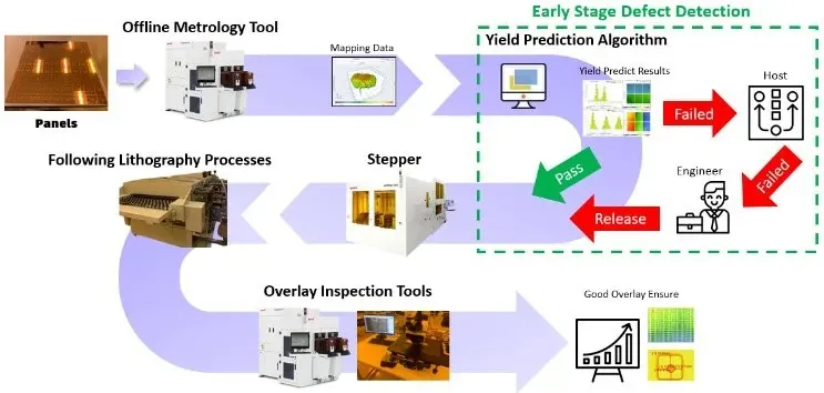
The article discusses a key manufacturing bottleneck in the race to produce more AI chips: lithography for advanced packaging. As AI packages get bigger and demand skyrockets, the industry is shifting from traditional wafer-based packaging to Fan-out Panel-Level Packaging (FOPLP). This method uses larger, rectangular panels instead of round wafers, packing in many more chips per substrate and significantly reducing costs. The core challenge is distortion: these massive panels warp and bend during production, causing tiny misalignments between chip layers that can kill yields. To fight this, engineers must find a "sweet spot" between using simple global corrections (fast but sloppy), more precise zone or die-by-die corrections (accurate but slow), or a middle-ground site-by-site approach. The takeaway is that the future of affordable AI hardware depends on solving this distortion puzzle, turning a promising packaging technology into a reliable, high-volume manufacturing process.
Read the original at semiengineering.com
Satirical commentary on real tech news, summarised with AI. Read the original source for the facts. How ZeroDaily works