
The Tiny Bugs That Could Shatter Your Next Superchip
Original headline: Shrinking Hybrid Bonding Pitches Push Inspection Limits — semiengineering.com
More in Semiconductor and chip news
As the tech industry races to cram more power into smaller packages, hybrid bonding has emerged as a key technique. This process directly fuses chips together at the microscopic level, enabling blistering speeds and efficiency for things like next-gen AI hardware and memory. However, the very thing that makes it so powerful—incredibly tight, sub-9-micrometer connections—is also its greatest weakness.
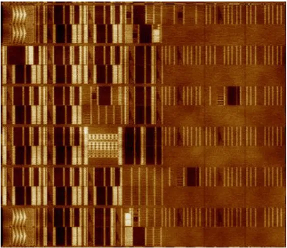
To make a reliable bond, the surfaces must be atomically flat and perfectly clean. A speck of dust 50 nanometers wide—thousands of times smaller than a human hair—or a microscopic scratch can cause a catastrophic delamination, ruining the entire chip stack. The article details the intense metrology arms race, where manufacturers are pushing optical inspection, X-ray, and atomic force tools to their limits to detect these 'killer defects' buried deep inside bonded chips. The takeaway: the future of high-performance computing hinges on our ability to see and control the invisible.
Read the original at semiengineering.com
Satirical commentary on real tech news, summarised with AI. Read the original source for the facts. How ZeroDaily works